
ADVANCED MATERIALS · ENGINEERING & RESEARCH
Semiconductor Wafers, Substrates & Precision Materials
Semiconductor materials, optical crystals and precision components for engineering, research and industrial applications.
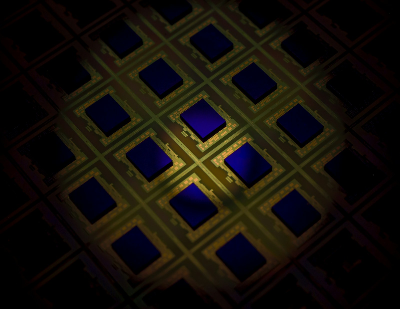
OUR MATERIAL PORTFOLIO
Five Specialized Product Families
From silicon carbide and sapphire to silicon, quartz and advanced ceramics, explore the materials behind precise engineering applications.
 01
Silicon Carbide Wafers & Substrates
4H-SiC, 6H-SiC, epitaxial and specialized substrates.
 02
Sapphire Materials & Components
Crystal wafers, optical windows, domes and precision tubes.
03Silicon & Specialty Wafers
Silicon, SOI, thermal oxide and compound wafers.
 04
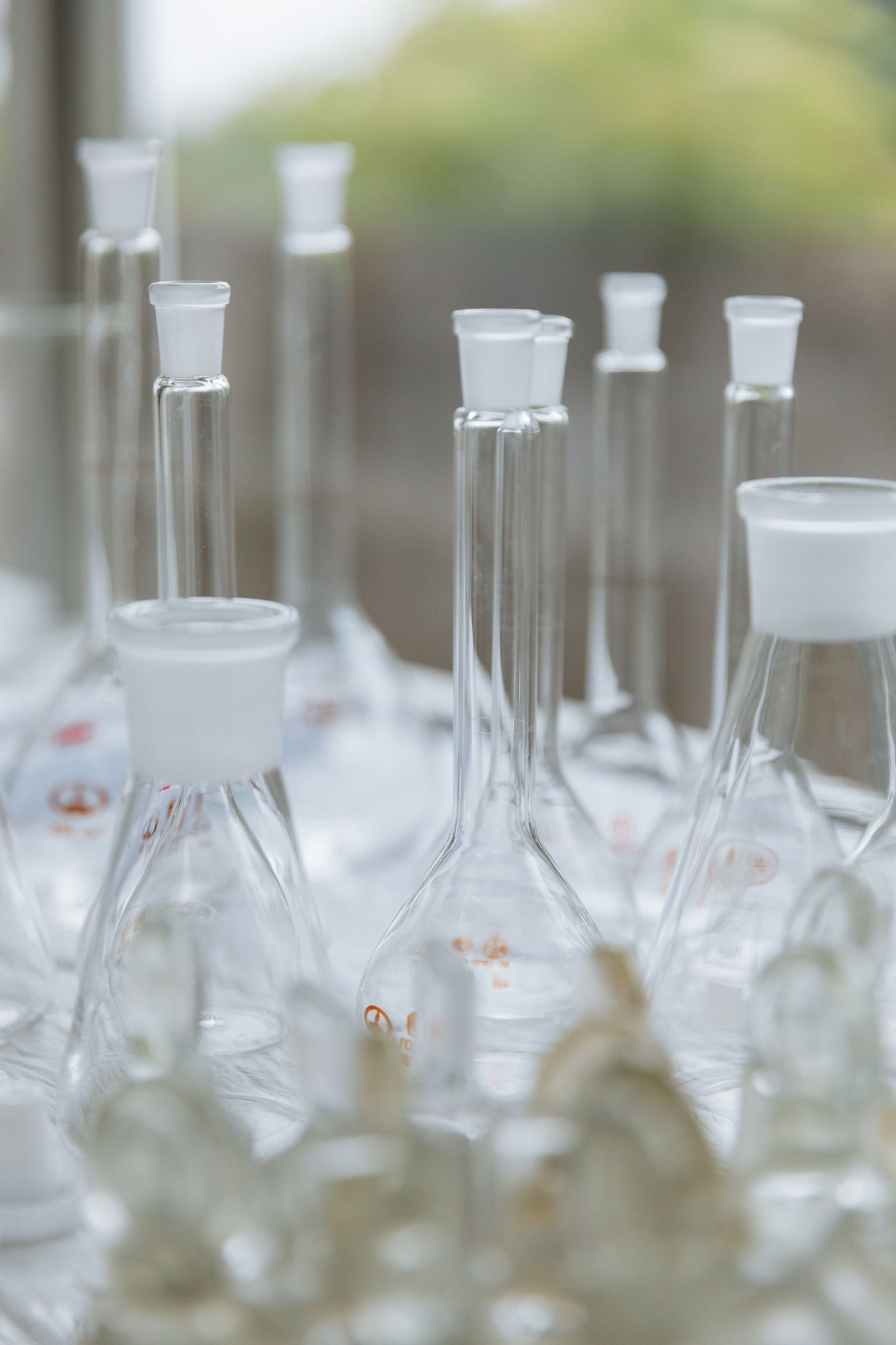
Quartz & Glass Components
High-purity fused quartz and technical glass parts.
 05
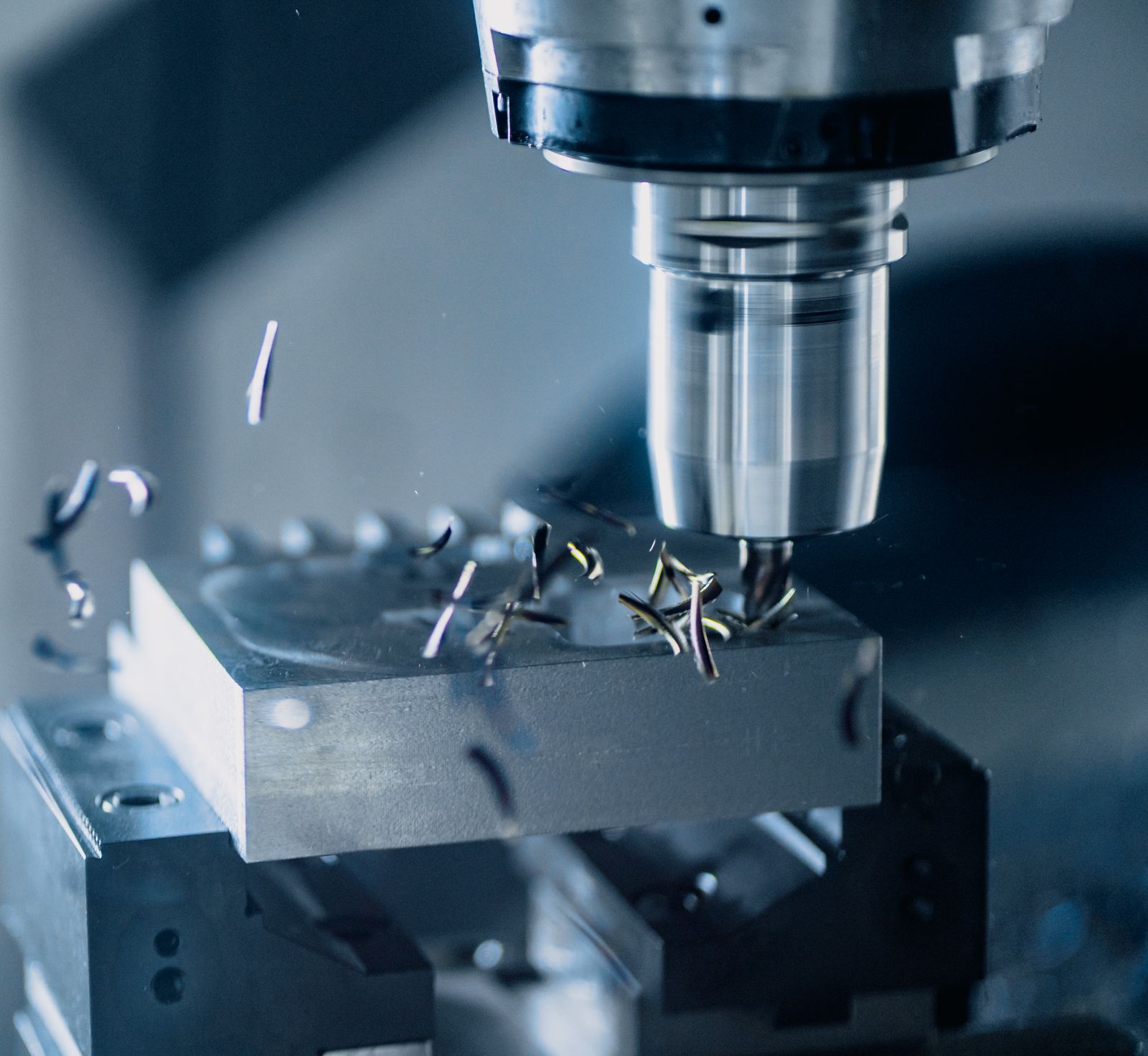
Advanced Ceramics & Wafer Handling
Technical ceramics and wafer handling components.
MATERIAL SELECTION
Define the right substrate before procurement
Material grade is only the starting point. A useful engineering request also defines size, thickness, crystallographic orientation, electrical characteristics, surface preparation, inspection criteria and end application.
For optical or equipment components, engineering drawings may further specify clear aperture, hole geometry, concentricity, flatness, edge finish and surface quality.
- Wafer and substrate specification review
- Optical crystal and machined-component discussions
- Quality documentation requirements agreed by order
ABOUT WEGITEK
Shanghai-based material sourcing with a specification-first approach
Shanghai Weijite Materials Technology Co., Ltd. provides a central inquiry point for advanced material requirements in semiconductor, optical, laboratory and industrial contexts.
Our catalog is organized to help engineering buyers identify the relevant material family and submit actionable specifications. Available grades, tolerances, delivery options and manufacturing routes are confirmed individually before any binding quotation.
About Our Company →
APPLICATION CONTEXT
Applications We Discuss
Explore how process and device requirements influence material selection.
Power Electronics
Wide-bandgap substrates and electrical specifications.
Explore →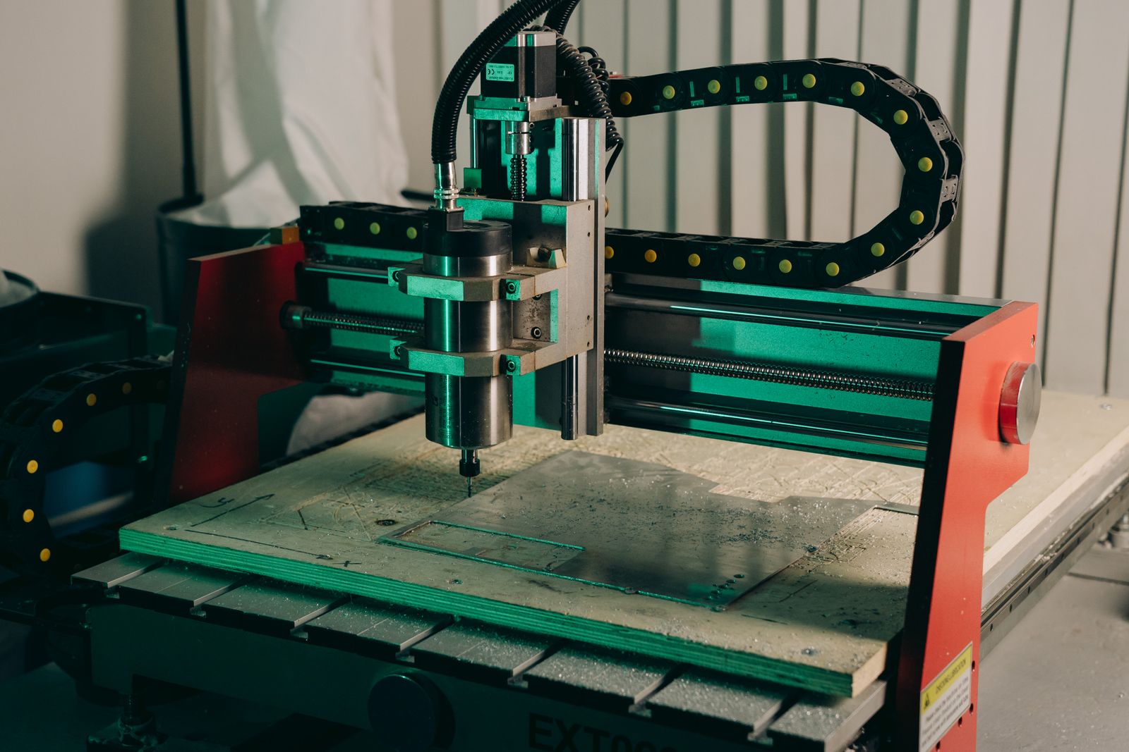
Semiconductor Equipment
Thermal-process quartz, ceramics and handling parts.
Explore →Photonics & Optics
Sapphire windows, crystals and optical surface requirements.
Explore →MEMS & Sensors
Silicon and SOI structures for microfabrication.
Explore →Advanced Packaging
Technical glass and carrier geometry considerations.
Explore →
University & R&D
Small-volume research and custom material specifications.
Explore →PROJECT INQUIRIES
Share your drawing or wafer specification.
Material, size, quantity, polishing and inspection criteria help our team discuss the right specification with you.